
INSULATING SUBSTRATE
Solution
Structure proposal by using unique
stress relaxation technology
Challenge
Hope to improve reliability of the power module
- Deal with minimization and increasing power density of power module, need to ensure bonding reliability under the more severe operating condition.
- In terms of developing power module, considering heterogeneous material (multi-material), but don't know whether combination is suitable.
Solution Overview
Lately, dealing with enlargement of heat generation density due to increase of die power density, insulating substrate for xEV (X Electronic Vehicle) and the other application's power conditioning invertor use thicker copper circuit material which has high heat coefficient in order to reduce heat resistance.
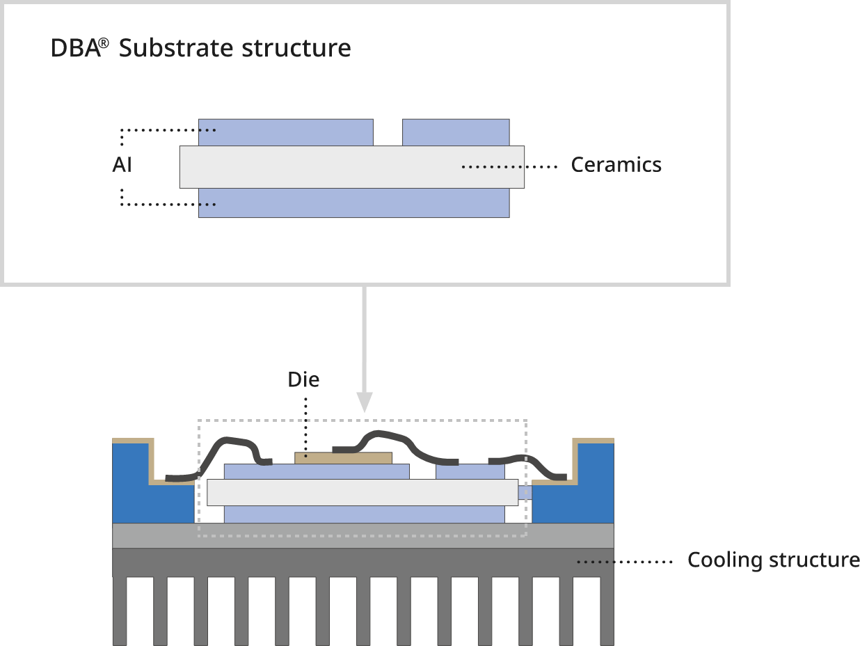
We are manufacturing and providing extremely high reliable power electric insulating substrate “DBA® Substrate” (“Direct Bonded Aluminum Substrate”) mainly use for xEV application which is ceramic substrate bonded with high purity aluminum circuit pattern on both top and bottom side. We enhanced functionality of bonding technology which is core technology from “DBA® Substrate” to work on research and development of new power electric insulating substrates and bonding materials. Until now, we developed DBA® Substrate integrated with aluminum heat sink which is bonded at low temperature.
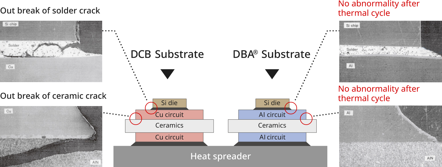
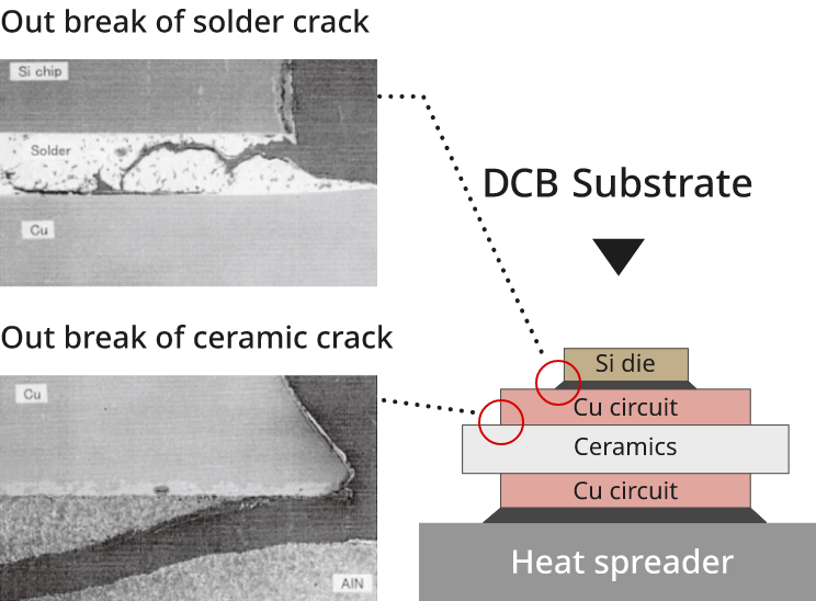
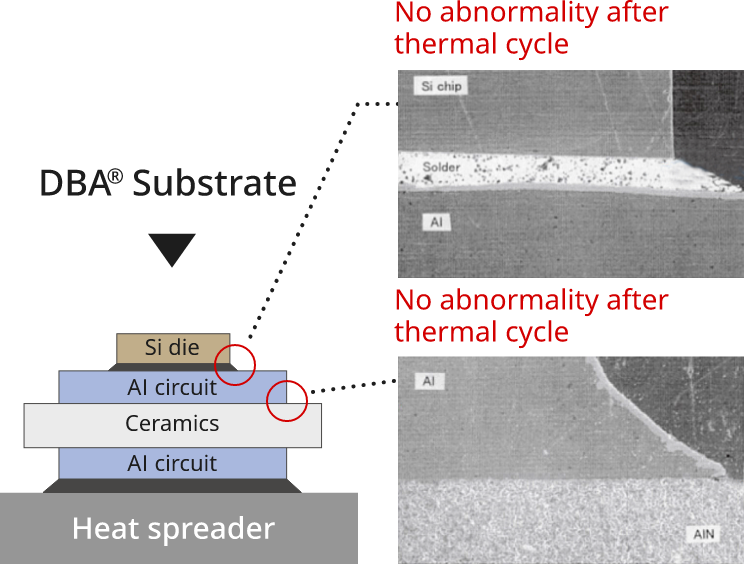
■ Comparative thermal cycle test of copper circuit substrate and DBA® Substrate (-40~125℃, 2500cycle)
Effect
-
Before
Despite applying silicon nitride which is high strength ceramic for insulating substrate, there is a limit to the maximum thickness of copper circuit material, and if add more copper circuit material thickness, it is difficult to make product due to declining of reliability (ceramic substrate will be more breakable).
-
After
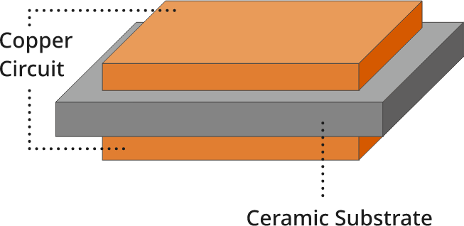
Combination of our interfacial bonding technology and metal processing technology, we succeeded to develop DBAC® Substrate which has pure aluminum stress relaxation layer in between ceramic substrate and copper circuit material.
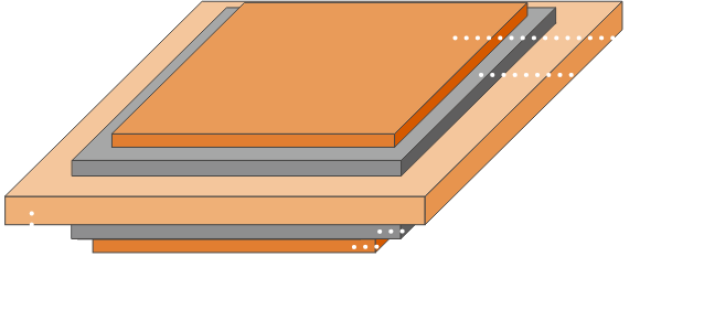
DBAC® Substrate has better bonding reliability than conventional insulating substrate which is made of copper circuit material on ceramic substrate (AMB Substrate, DCB Substrate). This development enable us to form thicker copper circuit more than ever.■ Double side copper bonded structure
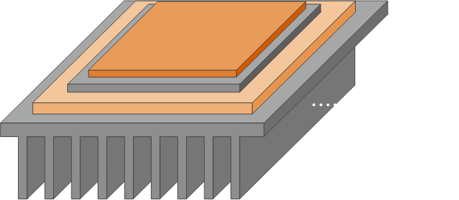
■ Heat sink integrated structure
ADVANTAGE
-
ADVANTAGE01
Owing to our original interfacial bonding technology, you can realize thicker copper insulating substrate.
-
ADVANTAGE02
Owing to our original interfacial bonding technology, you can improve bonding reliability.
-
ADVANTAGE03
Owing to strong thermal cycle tolerance insulating substrate, you can reduce the number of mounted insulating substrate.
OTHER SOLUTIONS
Other solutions for insulating substrate
-
INSULATING SUBSTRATE
Hope to reduce the thermal resistance of the power module
-
INSULATING SUBSTRATE
Hope to realize an efficient cooling structure
Other related solutions
-
AuSn PASTE
Hope to flexibly change the thickness and shape of AuSn
-
THERMISTOR SENSOR
Want a heat-resistant product compatible with SiC power semiconductors
-
THERMISTOR SENSOR
Hope to measure sudden temperature changes with good response
-
THERMISTOR SENSOR
Hope to discuss the structure and shape of the sensor
This solution utilizes
Mitsubishi Materials' insulating substrate.
( Responsible Dept.: Monozukuri and R&D Strategy Dept.)

