- Home
- Products & Business
- Electronic Materials and Components Business
Electronic Materials and Components Business
ADVANCED PRODUCTS COMPANY
Delivering Outstanding Development Skills and the On-Site Capabilities to Win out in the Business world
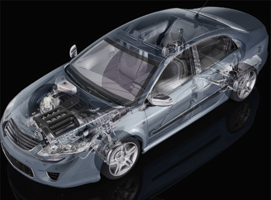
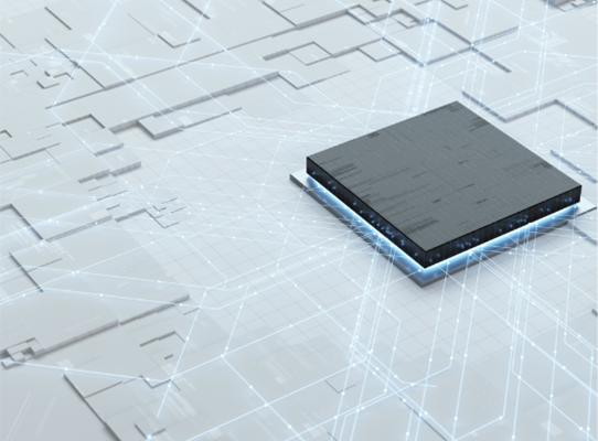
The progress in IT and electronics technologies has made our lives significantly more convenient through such items as personal computers, smartphones and tablet devices, not to mention automobiles and home appliances. Our Electronic Materials & Components Business supplies the electronics industry with unique, high-value-added products made from our distinctive materials.
Business Summary
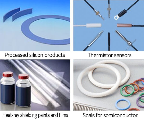
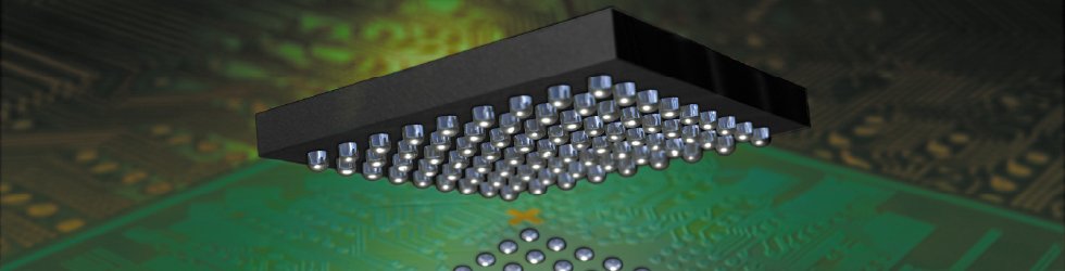
Our Electronic Materials and Components Business have a lineup of products such as processed silicon products for semiconductor equipment, lead frames, sealing materials, low-alpha solder plating chemicals, thermistor sensors for automobiles, and heat-ray shielding paints. We have multiple products with the world's No.1 market share. Our business is composed of five divisions: functional materials, electronic components, chemicals (Mitsubishi Materials Electronic Chemicals Co., Ltd.), seals (Mitsubishi Cable Industries, Ltd.), and semiconductor lead frames (Gotoh Manufacturing Co., Ltd.).
Targets and Strategy
Aiming to Remain a Highly Profitable Business Entity with Products That Have a Leading Share of World Markets
In Advanced materials division, we focus on semiconductor field to further expand our sales of low-alpha ray soldering materials and processed silicon products.
In Electronic components division, we are reinforcing our manufacturing and sales structures in line with the growing prevalence of energy-saving air conditioners in emerging markets.
Topics
Developed a "Square Silicon Substrate" for Semiconductor Packages
- 600 mm-square rectangular silicon substrate, one of the world's largest -
 Figure 1: Appearance of square silicon substrate (size example 510 mm x 515 mm x 0.8 mm) (right)(Left: 300 mm-dia. single-crystal silicon wafer (for size comparison))
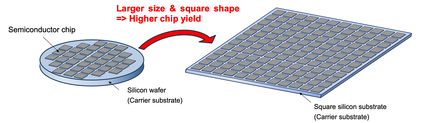 Conceptual diagram of semiconductor chips mounted on carrier substrate
Mitsubishi Materials Corporation has developed a "square silicon substrate," one of the world's largest rectangular-shaped silicon substrates that achieves high flatness and low surface roughness.
Next-generation semiconductor packages that employ chiplet technology, which has been attracting attention in recent years, are becoming increasingly larger, with sizes now up to about 100 mm square. In the semiconductor package manufacturing process, there is a problem with wafer-level packages (WLPs) that use a conventional 300 mm-dia. silicon wafer, etc. as a carrier substrate onto which semiconductor chips are placed. The problem is that packages cannot be efficiently fitted onto the wafer substrate because of the small area and circular shape of the wafer.
To solve this problem, MMC has developed a large-area, rectangular-shaped "square silicon substrate" by combining the casting technology for large silicon ingots, which the MMC Group has developed over many years, with MMC's proprietary processing technology.This "square silicon substrate" will contribute to improving productivity in the semiconductor field in several ways including its use as a carrier substrate in the semiconductor manufacturing process and its application as an interposermaterial for semiconductor packages.
History
The Electronic Materials & Components Business Company conducts business in four divisions: advanced materials, chemical products, electronic components, and seals.
Advanced Materials
| 1982 | Commenced production of precision rolled products at the Osaka Refinery |
|---|---|
| 1989 | Established the Sanda Plant |
| 2004 | Established the Shizuoka DBA Center |
| 2012 | Established MMC Electronic Materials Taiwan Co., Ltd. (predecessors MMC Electronics Taiwan Co., Ltd., established in 1995 and MUE Materials Taiwan Co., Ltd., established in 2006) |
Chemical Products
| 1991 | Established JEMCO Inc. (predecessors Tohoku Fertilizer Corp. established in 1938, Japan Electronic Metals Corp. established in 1959) |
|---|---|
| 2009 | JEMCO Inc. changed name to Mitsubishi Materials Electronic Chemicals Co., Ltd. |
Electronic Components
| 1983 | Launched ceramics plant |
|---|---|
| 1987 | Established MMC Electronics (Thailand) Ltd. |
| 1993 | Established MMC Electronics (M) Sdn. Bhd. |
| 2014 | Established MMC Electronics Laos Co., Ltd. |
Seals
| 1907 | Established Nippon Densen Manufacturing limited partnership company |
|---|---|
| 1986 | Changed name to Mitsubishi Cable Industries, Ltd. |
| 2010 | Became a wholly owned subsidiary of Mitsubishi Materials Corporation |
GOTOH MFG Co., Ltd.
| 1925 | Established Gotoh Shokai |
|---|---|
| 1967 | Changed name to Gotoh Manufacturing Co., Ltd. |
| 2020 | Became a member of the Mitsubishi Materials Corporation group |
Products

Mitsubishi Materials
Thermal Management
Solution for xEVs
Electronic Materials and Components Business Related Products
- Functional Materials
- Chemical Products
- Conductive Filler and Paint
- Solar Heat-ray Shielding Paint
- Titanium Black
- Organic fluorine products
- Electronic Devices
- Mitsubishi Cable Industries, Ltd.
- Sealing products
- Gotoh Manufacturing Co., Ltd.
- Semiconductor lead frames
Major Affiliated Companies
- Mitsubishi Cable Industries, Ltd.Production and sales of sealing products
- Mitsubishi Materials Electronic Chemicals Co., Ltd.Production of chemical products
- GOTOH MFG Co., Ltd.Production and sales of Semiconductor lead frames
Related Websites
List of Offices
- Sanda Plant
- Ceramics Plant
- Technology Dept. Semiconductor New Technologies & Materials Business R&D Center