- Home
- Products & Business
- Research & Development
Research & Development
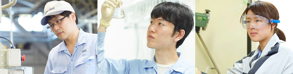
To strengthen the competitiveness of the Group's businesses and create new businesses, the Corporate Development function is led by R&D Strategy Division, which aims to establish an organization capable of delivering trusted value to customers—from research and development through to mass production and commercialization.
Organization of R&D Strategy Division
R&D Strategy Division concentrates its resources on technology and business development in the fields of the circular economy and GHG reduction, in line with the Group's management policy, "Creating the Future through Resource Circulation."
Through these efforts, the Division contributes to the growth and expansion of Mitsubishi Materials Group's resource circulation business for the future.
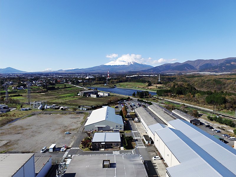
Mission, Vision and Values
Mission
Bringing together global knowledge, transforming technology into business, and supporting the growth of the Mitsubishi Materials Group
We actively gather knowledge on technologies, markets, and human resources not only from within the Group but from around the world. By leveraging the Group's technological strengths, we go beyond academic research and prototypes to deliver tangible value to society and customers.
These outcomes are then connected to business divisions, sites, and future growth domains, supporting the sustainable growth of the entire Group.
Vision
Act with integrity and respect. Challenge "Beyond the Border." Contribute to the world at the forefront.
We comply with laws and rules and act fairly at all times, while respecting both internal and external partners. By doing so, we continuously challenge "Beyond the Border" without being constrained by existing domains.
We aim to create and acquire cutting-edge technologies, maintain top-class technological capabilities, and generate technologies and businesses that contribute to the world by addressing social challenges and customer value from a global perspective.
Values
Driving innovation through expertise, dialogue, and collaboration
Each individual continues to refine their expertise and technical capabilities as the foundation of their work. By engaging in dialogue across disciplines, we create new value and systems that go beyond incremental improvements and conventional research.
Development Policy and Strategies
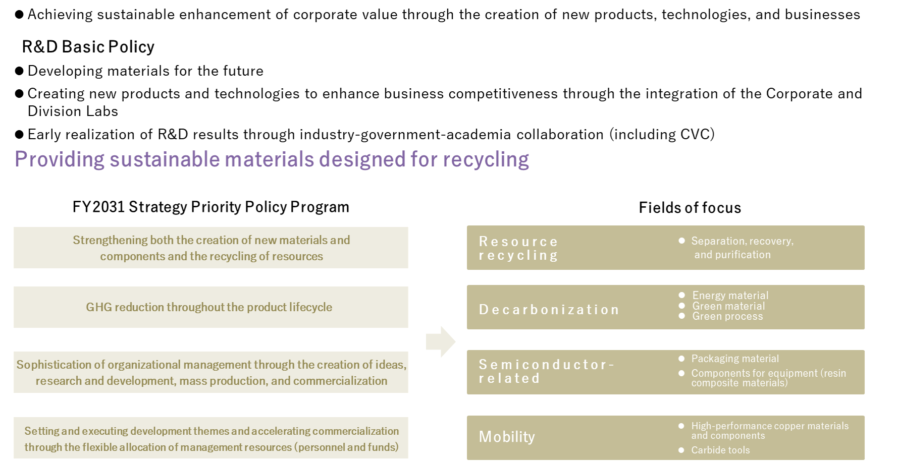
We accelerate idea generation, business validation, and commercialization through collaboration with business divisions and open innovation.
Policy
Creating new businesses and technologies in the circular economy and GHG reduction fields
Strategies
Strengthening our foundations in recycling and GHG reduction technology
Creating new materials to contribute to the circular economy
Advancing the creation of new businesses through the application of open innovation
Topics
Mitsubishi Materials Identifies Dopants that Improve Visible-Light Photocatalyst Performance Using Materials Informatics
Mitsubishi Materials Corporation ("MMC") announces that its Materials Informatics (MI) technology has been used to identify dopant elements that enhance the performance of a newly developed visible-light-responsive photocatalyst. The work, conducted through a collaboration with the Mitsubishi Materials Sustainability Innovation Collaborative Research Cluster Project in Institute of Science Tokyo, has been published in the Journal of the American Chemical Society.
The MI-based screening process enabled the rapid selection of promising dopant candidates from a broad set of elements. Materials synthesized by the Institute of Science Tokyo using these candidates demonstrated improved hydrogen generation from water under visible-light irradiation.
The results indicate the utility of MI in reducing the time required for materials discovery and optimization. The technology is expected to support future development of artificial photosynthesis systems and hydrogen-related applications.
More details can be found on the Institute of Science Tokyo website:
URL: https://www.isct.ac.jp/en/news/njsnm11on9b7
MMC will continue to integrate MI and digital technologies into its R&D framework and expand collaboration with academic institutions to accelerate materials development.
R&D on Recycling Used Cables Generated by Railroad Operations to Begin on April 1
- Aiming to establish a system for reducing waste by recycling copper and coating materials -
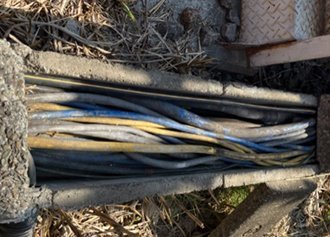 Signal cables placed along a track
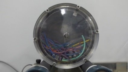 Separation of coating materials swollen by an organic solvent
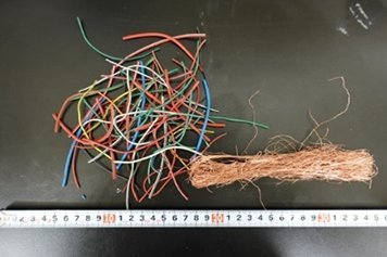 Copper wires and coating materials after separation
by the combined plastic swelling and ball milling method
The four parties—Tohoku University ("Tohoku University"), Tokyu Corporation ("Tokyu"), Tokyu Railways Co., Ltd. ("Tokyu Railways") and Mitsubishi Materials Corporation ("MMC")—will commence research and development on the recycling of used cables generated by railroad operations ("R&D") on Tuesday, April 1, 2025. This R&D has been selected for the FY2025 Environment Research and Technology Development Fund of the Environmental Restoration and Conservation Agency (ERCA) and will be carried out over three years, concluding in March 2028.
This R&D project uses cables from electrical facilities and signal cables along the tracks of Tokyu Railways, which are currently disposed of, as model cables to develop a combined plastic swelling and ball milling method ("Technology") for separating the cables into copper wires and coating materials. This Technology applies the separation principle of plastic swelling followed by separation through moderate impact from ball milling*, a method that Tohoku University has pioneered and developed in collaboration with MMC. While the cables used in this project have excellent strength to withstand the harsh conditions typical of railroads, the coated wires are thin. Existing coated wire treatment technologies make it difficult to separately sort copper wire and the coating materials to a high purity. As a result, the materials that can be recovered as recyclable resources from used cables are limited. Tokyu Railways generates an average of approximately 10 tons of such used cables per year. We aim to recycle the copper wires and coating materials recovered using this Technology into recycled cables for use in the railroad industry, including Tokyu Railways. Furthermore, we will evaluate the ripple effects on the railroad industry in the future by quantifying the CO2 emission reductions and economic benefits brought about by recycling.
This R&D has been made possible through the collaboration of four parties: Tohoku University, which has pioneered the research and technological development of the combined plastic swelling and ball milling method for coated wires; Tokyu, which formulated its Environmental Vision 2030 in March 2022 to realize a decarbonized and recycling-based society and tackles waste reduction by 10% by 2030; Tokyu Railways, which aims to solve environmental and social issues through activities including new value creation and contribution leveraging its business characteristics to realize a decarbonized and recycling-based society through its railroad business; and MMC, which has advanced smelting and recycling technologies for copper and other nonferrous metals.
Through this R&D, cables from the railroad industry will be made recyclable as recycled cables, which can be applied not only to the railroad industry but also potentially to other industries in the future. Through this effort, we aim to establish a system that reduces and recycles waste as much as possible.
- *
- Separating principle of the combined plastic swelling and ball milling method involves immersing cables in an organic solvent, which causes the coating materials to expand (swell). Impacting the cables in this state with small metal balls or balls made of other materials allows for the separation of copper wires and the coating materials without damaging them. This process is called the "combined plastic swelling and ball milling method."
Developed an Ink for Electron Transport Layer Deposition That Improves the Power Conversion Efficiency of Perovskite Solar Cells
- Approximately 1.5 times higher power conversion efficiency than conventional inks achieved -
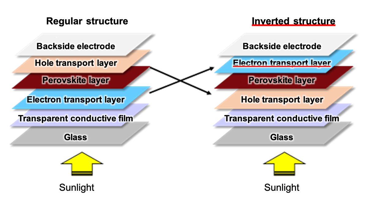 Figure 1: Schematic diagram of a perovskite solar cell
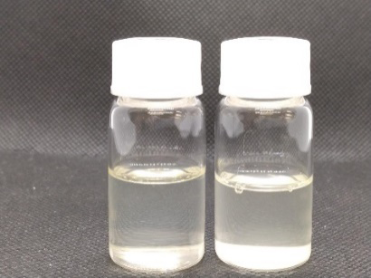 Figure 2: Newly developed tin oxide nano-ink
Mitsubishi Materials Corporation ("MMC") and EneCoat Technologies Co., Ltd. (headquartered in Kyoto, Japan; "EneCoat Technologies") have jointly conducted research and development of an electron transport layer, a component of perovskite solar cells, and developed a coating-type ink for film deposition that achieves approximately 1.5 times higher power conversion efficiency than conventional inks.
In recent years, perovskite solar cells have been attracting attention in the renewable energy field because of their high efficiency and low cost, as well as their light weight and flexibility, making them suitable for locations that did not allow easy installation. Durability and stability, which were previously considered issues, have also been improved through technological advances, and efforts toward commercialization are actively underway as the next generation of solar cells.
Perovskite solar cells have two types of structure depending on the material used for deposition: regular structure and inverted structure. The focus is now on the inverted structure for reasons of ease of manufacture and durability, and this structure requires the formation of a film called an "electron transport layer (*1)" on top of the perovskite layer without causing damage. Although fullerene (C60), a carbon-based material, has conventionally been deposited by a vacuum process, research and development on low-cost materials and new deposition methods are underway for commercialization. In addition, inks for the electron transport layer are required to prevent erosion on the perovskite layer, ensure ink dispersion (coatability), and provide uniformity and adhesion after deposition.
- (*1)
- Material that transports, from holes and electrons generated in the perovskite layer, only electrons to the current collector plate
The MMC Innovation Center has been commissioned by EneCoat Technologies, which was entrusted with the NEDO (*2) Green Innovation Fund Project, to develop an electron transport layer forming material that employs a coating-type process with excellent manufacturing cost, and has developed a new ink for film deposition.
- (*2)
- New Energy and Industrial Technology Development Organization
Although the coating-type process is non-vacuum and cost-effective, the solvent in the deposition ink damages the perovskite layer and, in a non-damaging organic solvent, nano-sized (of 10-9 m order) tin oxide (SnO2) agglomerates and does not adhere well to the perovskite layer, which posed an issue. The newly developed coating-type ink for the deposition of the electron transport layer coats the surface of tin oxide nanoparticles with an appropriate material to successfully disperse them in an organic solvent without agglomerating them, allowing formation of a dense coating film with sufficient adhesion to the perovskite layer. This allows the electrons produced from the perovskite layer to be efficiently transported to the metal electrode. By adopting this new technology, a high power conversion efficiency of 16.0%, approximately 1.5 times higher than that of conventional inks, has been achieved.
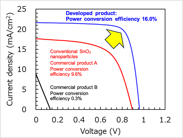
This achievement was presented at the Asia-Pacific International Conference on Perovskite, Organic Photovoltaics and Optoelectronics (IPEROP25), an international conference held on January 20, 2025, at Kyoto University Uji Campus.
MMC and EneCoat Technologies will continue to develop the process for applying the deposition ink, aiming for early commercialization for large-area perovskite solar cells.
This achievement was the result of a project (JPNP21016) funded by the New Energy and Industrial Technology Development Organization (NEDO), a national research and development agency.
Development of Sintering Copper Sheets Using Submicron Copper Particles
- Next-generation bonding materials enabling low-temperature, high-reliability bonding -
Mitsubishi Materials Corporation ("MMC") utilized its proprietary copper powder manufacturing technology to develop a new type of "sintering copper bonding material" using submicron copper particles, which enable sintering bonding at lower temperatures than conventional copper powders. The material is provided in the form of copper sheets for a wide range of applications.
■Background and purpose of development
High-power modules, such as those used in automotive and railway inverters, require low heat resistance, high heat dissipation capability, and long-term reliability at the joints due to the high-temperature operation and large current demands of semiconductor devices.
Conventionally, pressure-type sintering bonding materials primarily composed of silver have been widely used. However, they have posed challenges such as rising material costs due to soaring silver prices and the tendency for residual decomposition gases from organic solvents and resin components to remain during large-area bonding, leading to bonding defects.
Against this backdrop, MMC has been working to develop copper materials to resolve the challenges associated with conventional silver sintering bonding materials, namely high cost and reliability in large-area bonding. Specifically, MMC is working to advance material design by establishing an integrated development system that covers everything from the synthesis of copper powder to the design of sintering copper materials. As a result, MMC has developed submicron copper particles with a particle size of 100 to 200 nm, extremely low levels of metallic impurities, and high sinterability, due to our unique particle surface coating design. Using these particles, we have developed copper sheets that combine low-temperature bonding, large-area compatibility, and high reliability, serving as an alternative to conventional silver-based sintering materials.
■Features
MMC's proprietary sintering copper bonding material, which utilizes copper particles, possesses low-temperature sintering properties comparable to those of silver sintering materials despite being made of copper. This next-generation bonding material enables bonding at temperatures between 200 and 250°C within short durations under a nitrogen atmosphere. Copper sheets offer the following features:
- Excellent handling, enabling easy transport and setup. This eliminates the need for the printing and drying processes for organic components, which are essential for pastes, thereby shortening the process.
- Compared to paste types, it contains fewer organic components, enabling uniform bonding even on large-area power modules while suppressing void formation.
- Higher bonding quality and reliability due to its greater thickness compared to paste types.
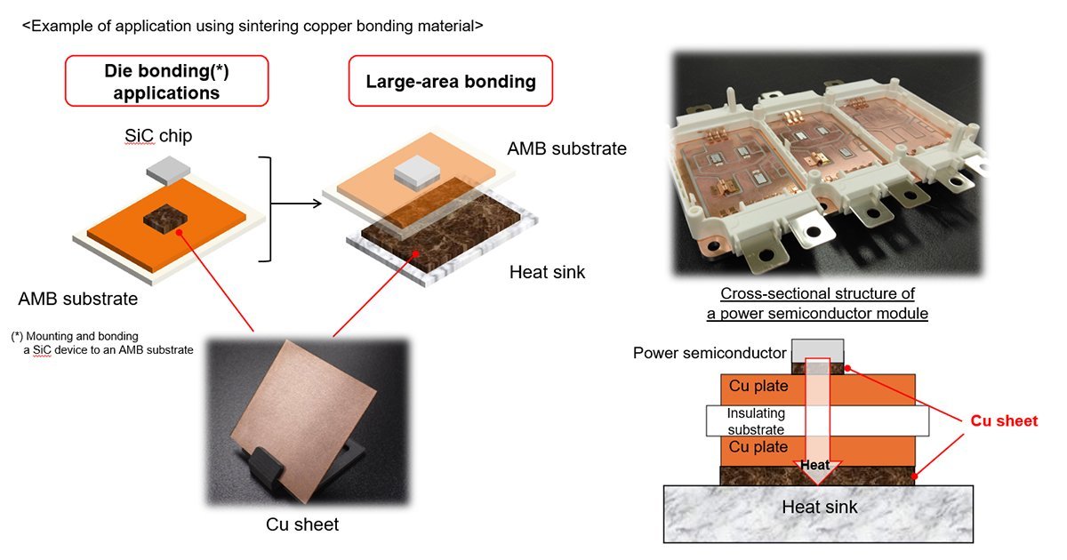
MMC plans to start providing copper sheet samples sequentially for various applications. We will contribute to improving the heat resistance, efficiency, and power saving of high-power modules for wide applications, including automotive and railway uses.
MMC Group has established "For people, society and the earth, circulating resources for a sustainable future" as Our Commitment, and strives to become a company dedicated to creating the future through resource circulation, while working to realize Our Commitment and enhance corporate value.
History
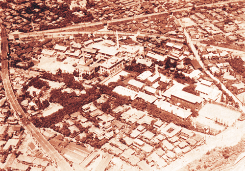 Mining Research Institute (At its start)
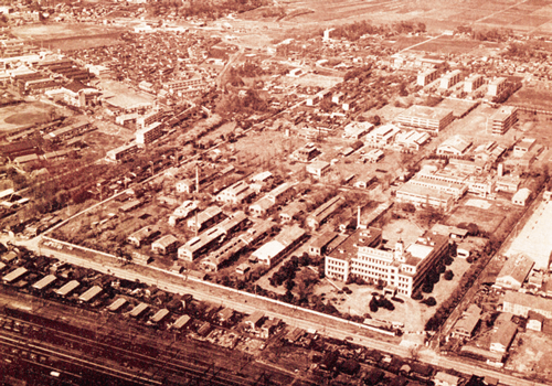 Mining Research Institute
(At the time of moved to Omiya)
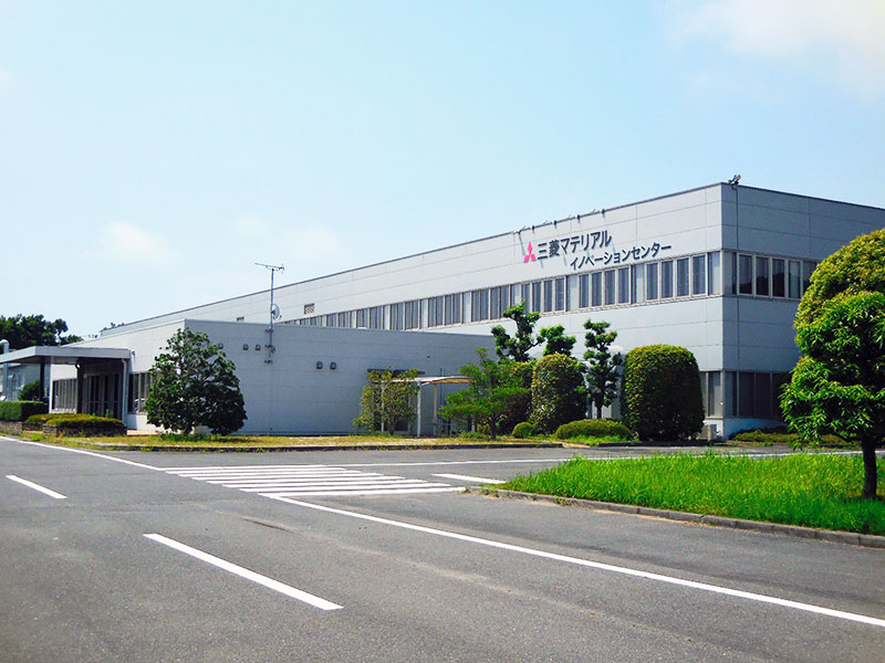
In 1917, Mitsubishi Goshi Kaisha established the predecessor to today's Innovation Center. Named the Mining Research Institute, this was Japan's first civilian research institute.
In 1939, the institute relocated to the city of Omiya, Saitama Prefecture. One of Japan's most preeminent research institutions for nearly a century, the Central Research Institute has engaged in research and development centered on materials and processes. Fields of application are diverse, including resources, energy, raw materials, basic materials, new materials, various types of products and even recycling. The institute generates synergies by making connections among these genres.
In 2001, we commemorated the dawning of a new century by constructing a new research wing in the city of Naka, Ibaraki Prefecture, and began a transition process that was completed in 2007. This year marked the relaunch of the Central Research Institute, operating branches in three regions: Onahama, Kitamoto and Omiya.
The name was changed from the Central Research Institute to the Innovation Center on April 1, 2022 in order to promote research and development and strengthening of manufacturing capabilities.
| 1917 | Established in Shinagawa, Tokyo, as the Mining Research Institute |
|---|---|
| 1939 | Relocated to the city of Omiya, Saitama Prefecture (now Omiya-ku, Saitama) |
| 1964 | Expanded fields of research, changed name to Central Research Institute |
| 1967 | Visited by the Showa Emperor and Empress |
| 1995 | Conducted organizational restructuring, changed name to the Sogo Kenkyujo |
| 2001 | Established the Omiya Research Center and the Naka Research Center within the Sogo Kenkyujo |
| 2007 | Conducted organizational restructuring, changed name to the Central Research Institute |
| 2022 | Conducted organizational restructuring, changed name to the Innovation Center |
R&D Review
No1.2022 Special Feature: Next Generation Vehicles
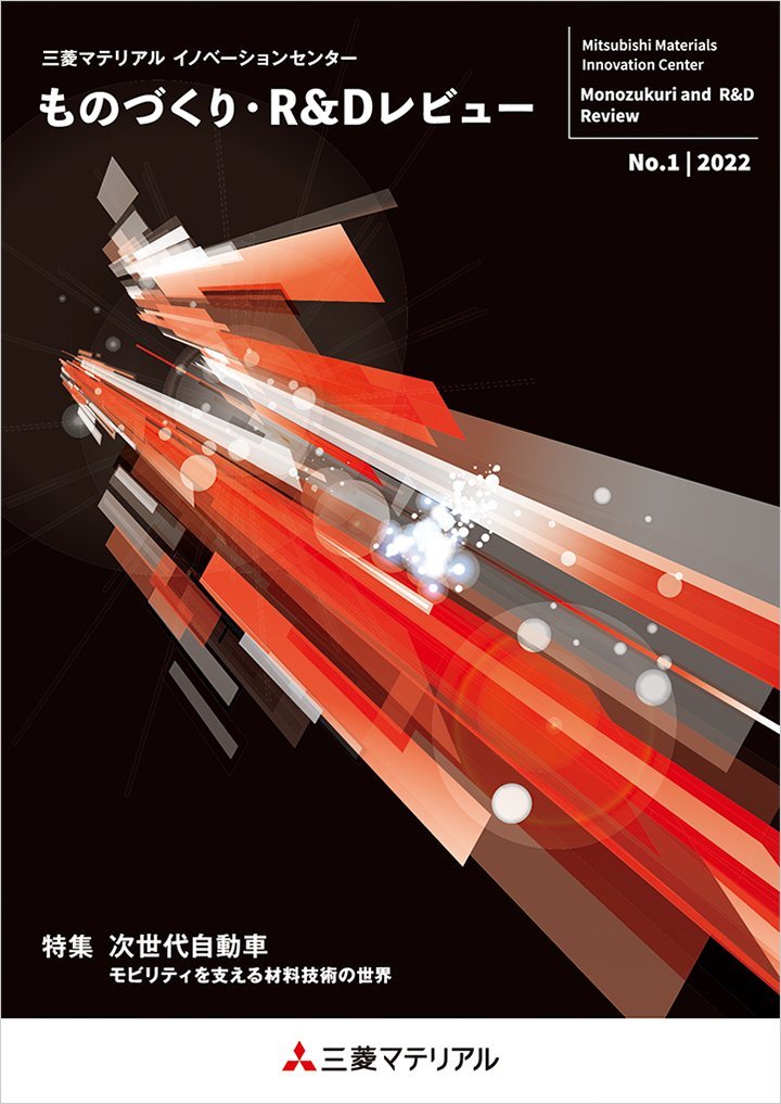 Monozukuri and R&D Review No1.2022 Cover Page
Special Feature: Next Generation Vehicles
- cBN Tools and Wear Mechanism in the Turning of Hardend Steel
- Development of Substrates for Power Modules with Suitable Material Properties
- Sintering Copper Paste for Power Device
- Development of Corrosion Protective Plating for Copper Terminal to Prevent Galvanic Corrosion of Aluminum Wire Harness
- Influence of Precipitates and Strain on Solder Heat Resistance of Cu-Fe-P Alloy
- Developments of Electro-Deposition Insulation Technology with a High Temperature Durability for Next Generation Vehicles