Advanced ProductsProducts Business Area
Business Overview
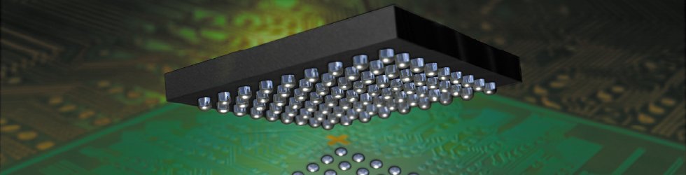
The Advanced Products business provides high value-added electronic materials and high-performance components based on proprietary materials technologies, with a focus on growth fields such as semiconductors, automotive applications (xEVs), healthcare, and electronic devices.
Its principal business domains include electronic chemicals, functional materials, copper and copper alloy products, and electronic components. The business offers integrated capabilities covering material design tailored to specific applications and customer requirements, as well as development, manufacturing, and sales. By combining materials technologies and processing technologies cultivated over many years, the business ensures a stable supply of products that require high levels of precision and reliability.
In addition, the business boasts multiple product lines with top-class global market shares and has earned strong recognition as a provider of key materials supporting the advancement of cutting-edge industries. Through continuous technological innovation and value creation, the business will continue to contribute to the resolution of social issues and the sustainable development of industry.
Business Objectives and Strategies
The Advanced Products business aims to establish a highly profitable business that achieves sustainable growth by focusing on fields expected to see further expansion, including semiconductors, xEVs (next-generation vehicles), and healthcare, while providing customers with products of enhanced added value.
To this end, the business will ensure a stable supply through expanded production capacity and promote the creation of new products and new businesses by further refining and integrating its core competencies. In addition, it will pursue market development through cross-functional collaboration among sales, development, and marketing under a key account framework, while strengthening customer engagement through the use of digital transformation (DX). Through the provision of high value-added products, the business seeks to contribute to the realization of a prosperous society.
Topics
Development of Square Silicon Substrate for Semiconductor Packages
— 600 mm-square rectangular silicon substrate, one of the world's largest —
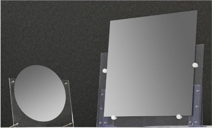 Figure 1: Appearance of square silicon substrate (size example 510 mm x 515 mm x 0.8 mm) (right)(Left: 300 mm-dia. single-crystal silicon wafer (for size comparison))
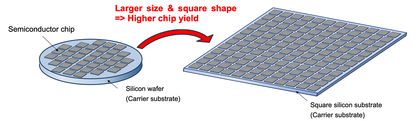 Conceptual diagram of semiconductor chips mounted on carrier substrate
Mitsubishi Materials Corporation ("MMC") has developed a "square silicon substrate," one of the world's largest rectangular-shaped silicon substrates that achieves high flatness and low surface roughness.
Next-generation semiconductor packages that employ chiplet technology, which has been attracting attention in recent years, are becoming increasingly larger, with sizes now up to about 100 mm square. In the semiconductor package manufacturing process, there is a problem with wafer-level packages (WLPs) that use a conventional 300 mm-dia. silicon wafer, etc. as a carrier substrate onto which semiconductor chips are placed. The problem is that packages cannot be efficiently fitted onto the wafer substrate because of the small area and circular shape of the wafer.
To solve this problem, MMC has developed a large-area, rectangular-shaped "square silicon substrate" by combining the casting technology for large silicon ingots, which the MMC Group has developed over many years, with MMC's proprietary processing technology. This "square silicon substrate" will contribute to improving productivity in the semiconductor field in several ways including its use as a carrier substrate in the semiconductor manufacturing process and its application as an interposer material for semiconductor packages.
History
| 1982 | Commenced production of precision rolled products at the Osaka Smelter & Refinery |
|---|---|
| 1983 | Launched the Ceramics Plant |
| 1987 | Established MMC Electronics (Thailand) Ltd. |
| 1989 | Established the Sanda Plant |
| 1991 | Established JEMCO Inc. (predecessors Tohoku Fertilizer Corp. established in 1938, Japan Electronic Metals Corp. established in 1959) |
| 1993 | Established MMC Electronics (M) Sdn. Bhd. |
| 2009 | JEMCO Inc. changed name to Mitsubishi Materials Electronic Chemicals Co., Ltd. |
| 2010 | Made Mitsubishi Cable Industries, Ltd. a wholly owned subsidiary |
| 2012 | Established MMC Electronic Materials Taiwan Co., Ltd. (predecessors MMC Electronics Taiwan Co., Ltd., established in 1995 and MUE Materials Taiwan Co., Ltd., established in 2006) |
| 2014 | Established MMC Electronics Laos Co., Ltd. |
| 2017 | Made LUVATA's SPECIAL PRODUCTS Division a consolidated subsidiary |
| 2020 | Made Gotoh MFG Co., Ltd. a wholly owned subsidiary |
Related Products
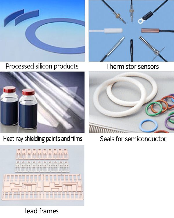
- Functional Materials
- Electronic Devices
- Chemical Products
- Mitsubishi Cable Industries
- Gotoh Manufacturing
- LUVATA
Major Affiliated Companies
- Mitsubishi Materials Electronic Chemicals Co., Ltd.Production of chemical products
- Mitsubishi Cable Industries, Ltd.Production and sales of sealing products
- Ryosei Kiko Co., Ltd.Production of electric wire and cable
- MMC Shanghai Co., Ltd.Sales of electronic components
- MMC Electronics (Malaysia) Sdn. Bhd.Production and sales of electronic components
- MMC Electronics (Thailand) Co., Ltd.Production and sales of electronic components
- GOTOH MFG Co., Ltd.Production and sales of Semiconductor lead frames
- Luvata GroupHolding company of the Luvata Group
Related Websites
List of Plants
- Sanda Plant
- Ceramics Plant
- Technology Dept. Semiconductor New Technologies & Materials Business R&D Center