News
August 21, 2024
Mitsubishi Materials Corporation
Developed a "Square Silicon Substrate" for Semiconductor Packages
- 600 mm-square rectangular silicon substrate, one of the world's largest -
Mitsubishi Materials Corporation ("MMC") has developed a "square silicon substrate," one of the world's largest rectangular-shaped silicon substrates that achieves high flatness and low surface roughness (see Figure 1 and Table 1).
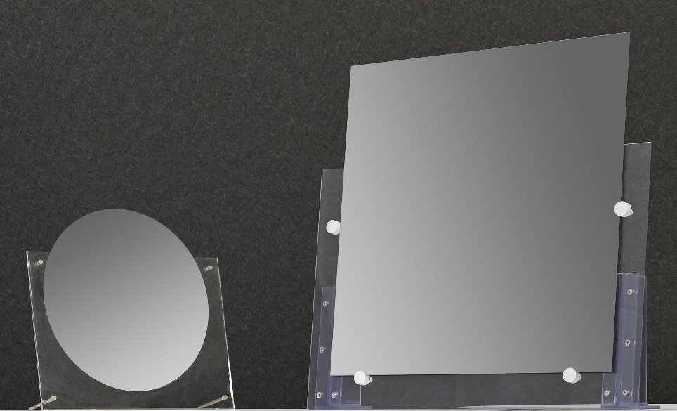
Figure 1: Appearance of square silicon substrate (size example 510 mm x 515 mm x 0.8 mm) (right)
(Left: 300 mm-dia. single-crystal silicon wafer (for size comparison))
Next-generation semiconductor packages(*1) that employ chiplet technology, which has been attracting attention in recent years, are becoming increasingly larger, with sizes now up to about 100 mm square. In the semiconductor package manufacturing process, there is a problem with wafer-level packages(*2) (WLPs) that use a conventional 300 mm-dia. silicon wafer, etc. as a carrier substrate onto which semiconductor chips are placed. The problem is that packages cannot be efficiently fitted onto the wafer substrate because of the small area and circular shape of the wafer.
To solve this problem, MMC has developed a large-area, rectangular-shaped "square silicon substrate" by combining the casting technology for large silicon ingots, which the MMC Group has developed over many years, with MMC's proprietary processing technology (see Figure 2).
This "square silicon substrate" will contribute to improving productivity in the semiconductor field in several ways including its use as a carrier substrate in the semiconductor manufacturing process and its application as an interposer(*3) material for semiconductor packages.
MMC Group has established "For people, society and the earth, circulating resources for a sustainable future" as "Our Commitment." We will continue to supply one-of-a-kind highly-functional materials and products and provide optimal solutions tailored to customer needs to strive toward realizing Our Commitment.
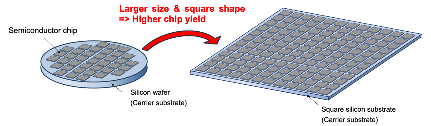
Figure 2: Conceptual diagram of semiconductor chips mounted on carrier substrate
(Click the picture to see the enlarged image)
- (*1)
- A next-generation semiconductor package is a composite component in which semiconductor devices and integrated circuits are encapsulated with resin, etc. to dissipate heat from the semiconductor devices, protect them from the outside, electrically connect them to the outside and improve their mountability on printed circuit boards.
- (*2)
- A wafer-level package is a semiconductor package that is completed by processing to the final step on a wafer substrate.
- (*3)
- An interposer is a substrate used for three-dimensional mounting of semiconductor packages to obtain conductivity of circuits on the front and back sides by means of through-hole electrodes.
[Overview]
As CPUs and GPUs for servers have become more sophisticated in recent years due to the spread of cloud services and AI, the adoption of next-generation semiconductor packages that use a technology known as "chiplets" is increasing.
Unlike conventional semiconductors, in which large integrated circuits are built into a single chip, chiplets are made by manufacturing multiple semiconductor chips separately and combining them into a single package. The semiconductor chips are connected by using a silicon interposer or forming a redistribution layer (RDL) composed of copper and resin (see Figure 3).
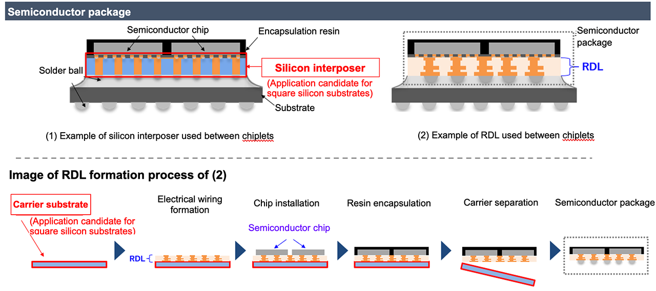
Figure 3: Conceptual diagrams of semiconductor packages and the RDL formation process
(Click the picture to see the enlarged image)
These packages are becoming increasingly larger, with size now up to about 100 mm square. In order to efficiently fit packages onto a carrier substrate, the carrier substrate must be made rectangular in shape and larger in size. It is technically difficult to make large substrates from single-crystal silicon materials, and a panel-level package(*4) (PLP), which uses a large glass panel, etc. as a carrier substrate, has been developed. However, glass materials have low rigidity and low thermal conductivity, which causes the problem of warpage due to uneven heat and thermal shrinkage during the heating process in RDL formation.
With the newly developed "square silicon substrate" used as a PLP carrier substrate, it has been confirmed that its characteristic high rigidity and high thermal conductivity can improve warpage, which has been a problem in the RDL formation process (see Figure 4).
Taking advantage of these characteristics, it is expected that a wide range of uses will be found for "square silicon substrates" in the semiconductor field in the future.
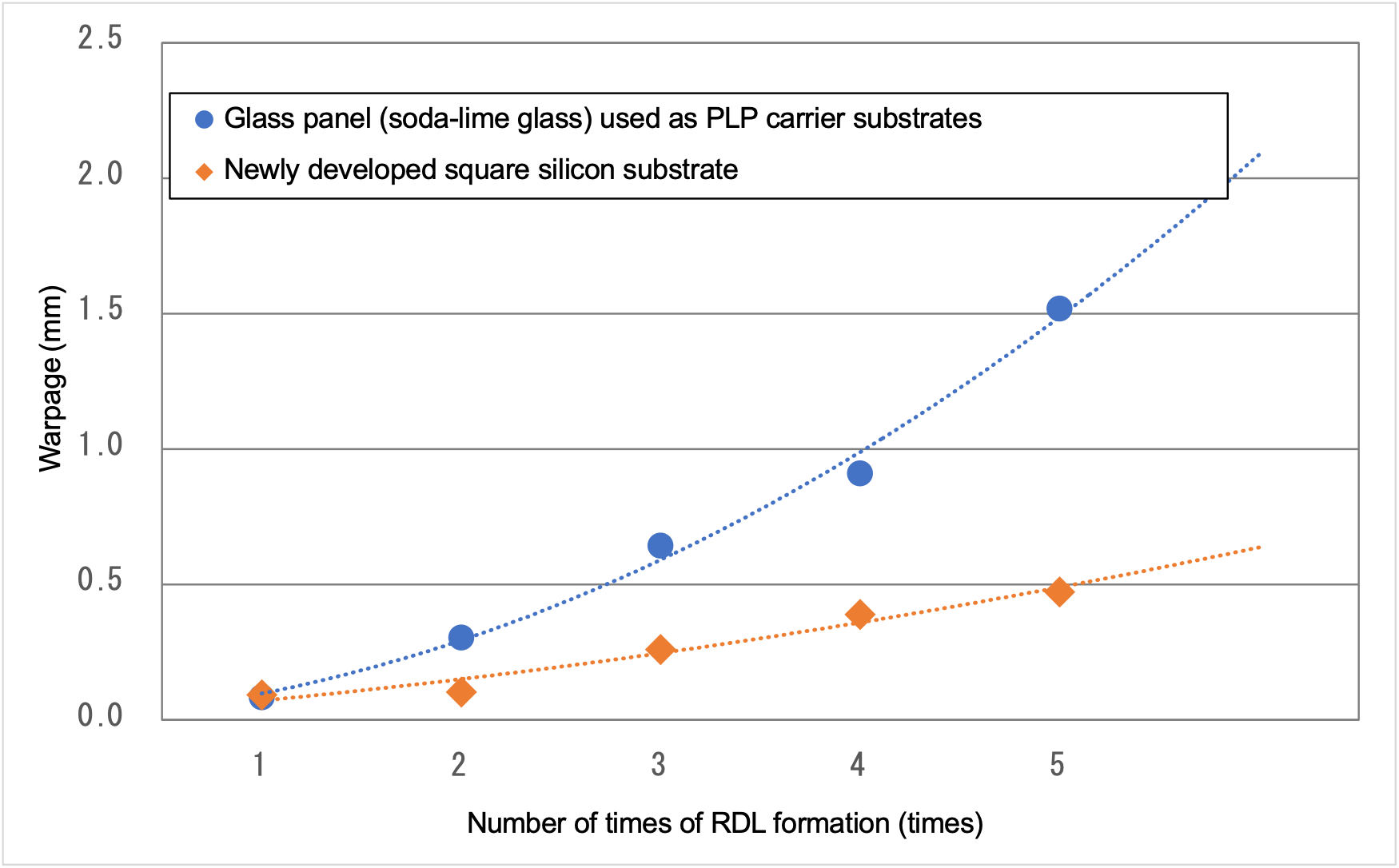
Figure 4: Number of times of RDL formation and amount of substrate warpage
Table 1: Overview of newly developed square silicon substrate
| Material | High-purity silicon | |
|---|---|---|
| Applicable size (square) |
Outer shape | 300 mm × 300 mm 510 mm × 515 mm 600 mm × 600 mm, etc. |
| Thickness | >0.8 mm | |
| Dimensional tolerance (peripheral) |
Outer shape | ±0.2 mm |
| Thickness | ±0.05 mm | |
| TTV (flatness) | <10 μm (experimental value) | |
| Surface roughness | Sa | <2 nm (experimental value) |
| Sz | <50 nm (experimental value) | |
(Note) The above values are typical values, not specifications.
- (*4)
- A panel-level package is a semiconductor package that is completed by processing to the final stage on a substrate larger than a wafer (such as printed circuit board or glass substrate).
<Contact details for inquiries>
Corporate Communications Dept.
+81-3-5252-5206