News
April 2, 2019
Development of Two Types of Sintering Bonding Materials for Next-generation Power Modules
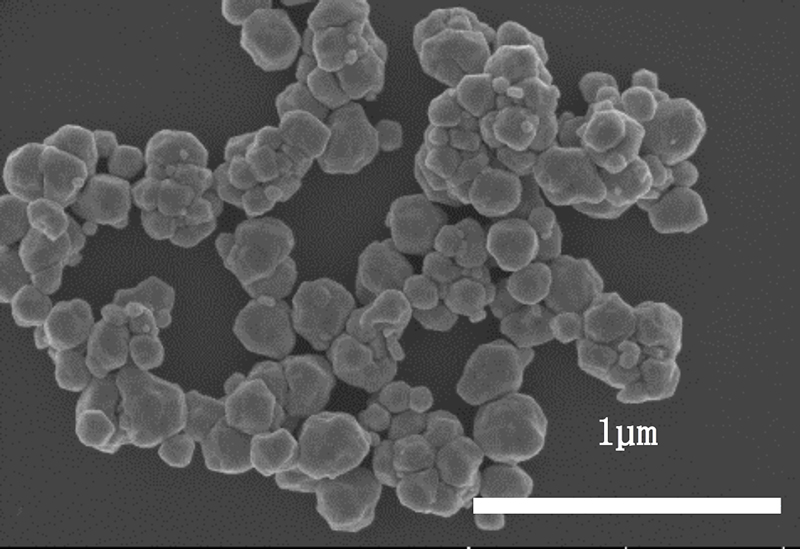
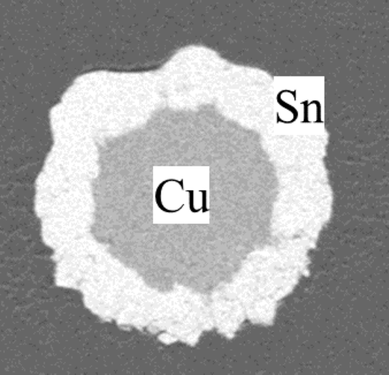
Mitsubishi Materials Corporation (President: Naoki Ono, Capital: 119.4 billion yen, "MMC") announced today that it has developed two types of sintering bonding materials (collectively "new products"), including a bonding material using low-temperature sintering submicron copper particles (Fig. 1, "sintering copper bonding material") and another bonding material using core-shell particles including copper coated with tin (Fig. 2, "core-shell bonding material").
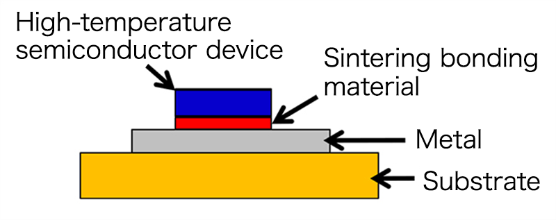
These new products are expected to be adopted for next-generation power modules such as high-output motor power control inverters for hybrid vehicles. With the accelerated spread of high-output motor power control inverter modules and the like, the use of high-temperature semiconductor devices (Fig. 3), including silicon carbide (SiC) and gallium nitride (GaN), capable of operating in high-temperature environments of 200℃ or greater has been expected to expand. However, in such high-temperature environments, lead-free solder, conventionally used as a device bonding material, is unable to be used because the melting point is around 200℃, meaning the heat resistance is insufficient.
To solve the above problem, MMC has developed two types of new products with different features. Both new products have an extremely high heat resistance and are capable of simultaneously solving problems that arise in conventional products.
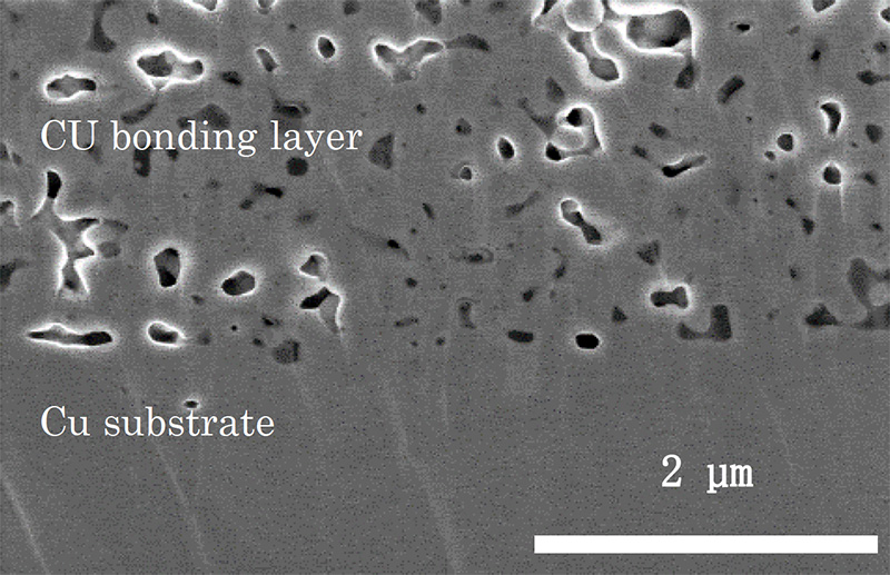
Conventional sintering copper bonding material requires reduction treatment with active gas for the removal of oxide film from the surface of copper powder. Our new products are usable for bonding at low temperatures and in an inert atmosphere, because they are coated with organic molecules that decompose at low temperatures.
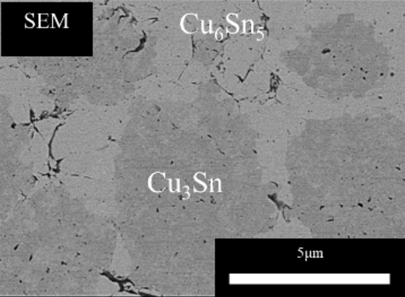
In addition, during the bonding of intermetallic compounds through liquid phase sintering, it has been conventionally problematic that heat treatment takes a long time. In contrast, the core-shell bonding material, one of the new products, implements bonding in a short amount of time, activating the reaction between tin and copper thanks to its core-shell structure.
| Sintering copper bonding material | Core-shell bonding material | |
|---|---|---|
| Particle properties | Copper: powder uniquely developed by MMC through reduction treatment on a slightly soluble copper compound | Intermetallic compound obtained by liquid phase sintering between copper and tin (Fig. 5): powder uniquely developed by MMC including copper particles coated with tin on the surface |
| Properties and functions | Usable for bonding at low temperatures and in an inert atmosphere (Fig. 4) |
Implements bonding in a short amount of time |
It is expected that the use of the new products will expand as sintering bonding material for next-generation power modules for which high heat resistance and high reliability are desired. The development of the new products is also scheduled to be presented at the 33rd Japan Institute of Electronics Packaging (JIEP) Spring Lecture Meeting to be held at Takushoku University Bunkyo Campus from March 11 to March 13, 2019.
In its long-term management policy, the MMC Group aims to become "the leading business group committed to creating a sustainable world through materials innovation, with the use of our unique and distinctive technologies, for People, Society and the Earth." Moving forward, the Group will continue to contribute to the development of the power apparatuses field through the development of products utilizing its unique, proprietary technologies.
 Click for enlarge
 Click for enlarge
 Click for enlarge
 Click for enlarge
 Click for enlarge
Official website of the 33rd Japan Institute of Electronics Packaging (JIEP) Spring Lecture Meeting:
https://web.jiep.or.jp/event/convention.html
[Related release]
Release dated January 11, 2017
Development of Sintering Bonding Material for Next-generation Power Modules
http://www.mmc.co.jp/corporate/ja/news/press/2017/17-0111.html
End.
March 6, 2019