News
August 31, 2018
W-Ti Sputtering Target for Barrier Films Developed, with Mass-Production Commenced in July
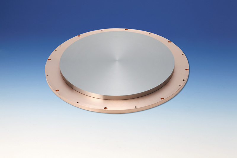
Mitsubishi Materials Corporation (President: Naoki Ono, Capital: 119.4 billion yen) announced today that the Electronic Materials & Components Company has developed a W-Ti (tungsten-titanium) sputtering target for barrier films supporting the semiconductor fine pitch process and commenced mass-production in July.
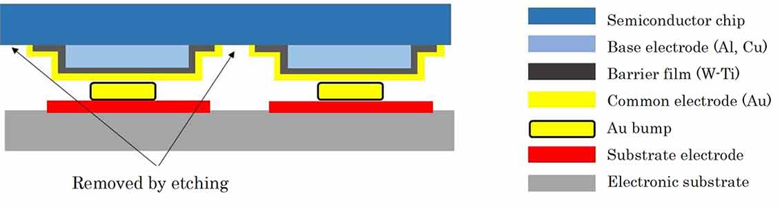
When mounting a semiconductor chip on an electronic substrate, Au (gold) bumps acting as spherical electrodes are formed on an Al (aluminum) or Cu (copper) base electrode (refer to the "junction cross-sectional view" below). However, as electronic devices are used at high temperatures more frequently, the more likely it is that electrical resistance will increase and adhesion will deteriorate, due to the mutual diffusion of the elements of the base electrode and Au bumps. Therefor, the mutual diffusion of the elements is normally prevented by using a barrier film (W-Ti film) formed by a W-Ti sputtering target between the base electrode and the Au bumps. The W-Ti barrier film is deposited on the whole surface of the semiconductor chip and the parts where the Au bumps will not be set will be removed by etching*. However, because the etching rate (the speed of barrier film being melted in etching) in the conventional barrier film is slow and difficult to control, users have been seeking for an etching rate that supports increased productivity in the semiconductor device mounting process and the semiconductor fine pitch process.
In order to meet this need of users, Mitsubishi Materials has been refining the accumulated knowledge of metallic composition design know-how and development experience of sputtering targets. As a result, the company managed to increase the etching rate of a generated barrier film by up to 60% from that of its conventional products and, moreover, achieved the capability to flexibly control the etching rate according to the customer's needs.
The recent movement towards the increase in functionality for smartphones and other devices has led to a narrower electrode intervals for semiconductor chips, increasing the need for fine-pitch junction. The development of W-Ti sputtering targets will contribute to increased productivity in the semiconductor device mounting process while enabling the support of the semiconductor fine pitch process.
Mitsubishi Materials has a vision of "becoming the leading business group committed to creating a sustainable world through materials innovation, with the use of our unique and distinctive technologies, for People and the Earth." Its Electronic Materials & Components Company will continue making contributions to society through the provision of unique and excellent electronic material products, anticipating market needs, and solutions.
- *Etching
- Molding or surface treatment technique using the corrosion action of chemical agents, etc.
 Click for enlarge
 Click for enlarge
July 25, 2018