News
November 17, 2017
World's Highest Level Solder Material with Alpha-Ray Emissions
Reduced Approximately 50% Developed, Mass Production Started
Mitsubishi Materials Corporation (President: Akira Takeuchi; Capital: 119.4 billion yen) announced today that its Electronic Materials & Components Company has developed the world's highest level solder material with alpha-ray emissions, which negatively affect the behavior of semiconductor devices, reduced by approximately 50% from the conventional product. Mass production has been underway since October.
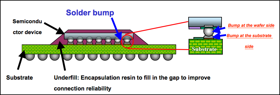
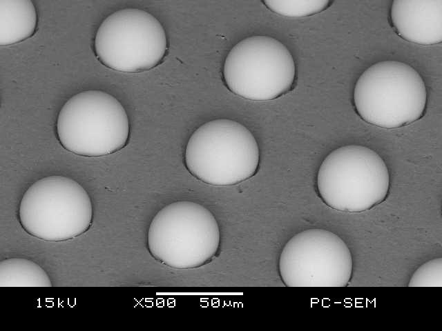
The solder material becomes spherical particles (hereinafter called "solder bump*1") when heated and joints a semiconductor device and a substrate, which constitute an IC chip. It also acts as electrodes between them (refer to "Cross-section View of IC Chip" below). One of the main ingredients of the solder material, which is the origin of the solder bump, is Sn (tin). It contains trace amounts of radioactive materials, from which alpha-rays are emitted. The emitted alpha-ray negatively affects the behavior of semiconductor devices and may cause a so-called software error (the phenomenon in which data in a memory is overwritten). To produce more reliable semiconductor devices, it is vital to use solder materials that emit fewer alpha-rays. Especially in recent years, demand has been growing for more reliable semiconductor devices that further reduce alpha-ray radiation.
To respond to these user needs, we have built on the alpha-ray dose reduction and management technologies that we have accumulated over more than 30 years, and succeeded in developing a "HULA*2"-grade solder material, which achieves 0.001 cph/cm2 (count per hour) or less. This is an advance from the conventional "SULA*3"-grade solder material, with alpha-ray radiation of 0.002 cph/cm2 or less.
New products containing the newly developed "HULA*2"-grade solder material will be added to some of our product lineups, such as Sn-Ag (silver) plating chemicals, Sn-Ag-Cu (copper) solder pastes, and Sn anodes*4.
In addition, in parallel with the development of the world's highest level "HULA"-grade solder material, we have accumulated more sophisticated alpha-ray analysis and evaluation technologies. In circumstances where mounting methods are diversifying, not only solder materials but also semiconductor package peripheral materials will be required to reduce its alpha ray radiation in the future. Given that, we will also apply the "HULA"-grade sophisticated alpha-ray analysis and evaluation technologies to our alpha-ray measurement services, which we have provided to users in the semiconductor industry in order to enhance our ability to provide solutions to users of the solder materials.
We have a vision of "Becoming the leading business group committed to creating a sustainable world through materials innovation, with the use of our unique and distinctive technologies, for People, Society and the Earth." Our Electronic Materials & Components Company will continue to contribute to the society by providing electronical materials and their solutions that pre-empt market needs.
- *1. Bump
- A spherical electrode used to connect the chip with the substrate in an integrated circuit.
- *2. HULA
- Hyper Ultra Low Alpha is a name of a new grade, which indicates that the radiation dose of alpha-ray is 0.001 cph/cm2 or less.
- *3. SULA
- Super Ultra Low Alpha is a name of the grade that indicates that the radiation dose of alpha-ray is 0.002 cph/cm2 or less.
- *4. Anode
- An electrode through which current (electrons) flows in (out) from (to) an outside circuit.
 Click for enlarge
 Click for enlarge
 Sn-Ag plating chemicals
 Sn-Ag-Cu/Sn-Cu solder pastes
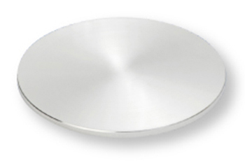 Sn anode
November 13, 2017