News
January 27, 2017
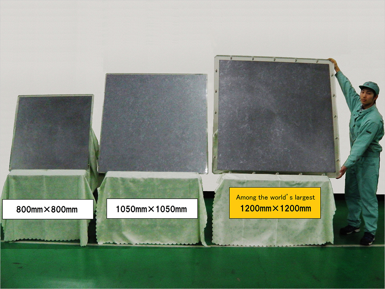
Technology Developed for Manufacturing Columnar Crystal Silicon, Among World's Largest
The Mitsubishi Materials Corporation (President: Akira Takeuchi; Capital: 119.4 billion yen) announced today that its Electronic Materials & Components Company has established the technology for manufacturing columnar crystal silicon that is among the largest in the world, harnessing the advanced knowledge on precision casting the company has cultivated over many years, in collaboration with Mitsubishi Materials Electronic Chemicals Co., Ltd. (President: Masami Koshimura; Capital: 2.6 billion yen), one of its consolidated subsidiaries. The practicality of the silicon has been remarkably improved by increasing the purity and reducing the internal stress, and the length of one side of the square exceeds 1,200 mm.
Columnar crystal silicon is polycrystalline silicon with a "columnar" crystal structure produced by growing silicon crystal in a unidirectional way and solidifying it. Silicon is not only brittle in quality, but also expands in volume during the solidification process: The physical property of being susceptible to fracture rapidly emerges if its size is enlarged. Mitsubishi Materials has utilized the advanced precision casting technology it has cultivated over many years to establish manufacturing technology that enables an increase in purity and reduction in internal stress, making it possible to reliably produce large-size columnar crystal silicon with remarkably improved practicality.
As a result of establishing the technology for manufacturing large columnar crystal silicon, Mitsubishi Materials expects that its use will expand in fields such as components for semiconductor manufacturing equipment (components for plasma etching device*1, soaking plate*2, and the like) and sputtering target materials, in which columnar crystal silicon has already been used. In recent years, demand for reducing impurities in semiconductor devices has increased with the miniaturization of semiconductors, and columnar crystal silicon has found application not only in the peripheral components of wafers, but also in larger components for which other materials have been used. In addition, substrates in flat panel display areas are becoming larger and there is a growing need for larger columnar crystal silicon for soaking plates used in the process of heat treating the substrate. As Mitsubishi Materials' large columnar crystal silicon has high purity and excellent workability, it should find application in a range of other product areas.
Mitsubishi Materials is scheduled to ship samples of the columnar crystal silicon by the end of fiscal year 2016. The Company welcomes visitors to Neo Functional Material 2017 held at Tokyo Big Sight from Wednesday, February 15 to Friday, February 17, 2017.
In its long-term management policy, Mitsubishi Materials promises that it will be "the world's leading business group committed to supporting recycling-oriented society through materials innovation with use of our unique and distinctive technologies." The Electronic Materials & Components Company and Mitsubishi Materials Electronic Chemicals Co., Ltd. will contribute to society by providing large columnar crystal silicon supported by its unique precision casting technology.
- *1
- Plasma etching device
A device to scrape a thin film-such as an oxide film on a wafer on which a circuit pattern is drawn-along the pattern with an etching gas in a plasma state, using a photoresist (a photosensitive chemical agent with the ability to withstand etching) - *2
- Soaking plate
A plate made of silicon that enables uniform heat treatment for substrates and the like, due to its narrower distribution of temperature on the surface
[Intended purposes]
Components for plasma etching device, soaking plate (for annealing furnaces and diffusion furnaces), susceptors (for CVD equipment), sputtering target material, and infrared lens
 Click for enlarge