News
October 23, 2014
Mitsubishi Materials Corporation
SCREEN Holdings Co., Ltd.
Mitsubishi Materials & SCREEN Semiconductor Solutions First in the MEMS Industry to jointly develop a Mass Production Technology for PZT Films Attains a productivity more than two times higher than conventional products
The Electronic Materials and Components Company (hereinafter referred to as “Mitsubishi Materials”) of Mitsubishi Materials Corporation (President: Hiroshi Yao) and SCREEN Semiconductor Solutions Co.,Ltd. (President: Tadahiro Suhara; hereinafter referred to as “SCREEN Semiconductor Solutions”), a group company of SCREEN Holdings, hereby announce the successful co-development of the MEMS industry's first mass production technology for PZT (lead zirconate titanate) piezoelectric films*1 used in Micro Electro Mechanical Systems (MEMS*2) devices.
1.Background of Development of this New Mass Production Technology
PZT films are functional-thin films with a piezoelectric effect, that are expected to enhance their utility in a wide range of MEMS devices, such as heads of inkjet printers, sensors and actuators for automotive use, energy harvesting devices for sensor network use, etc.
Mainly, there are two ways to form PZT films in semiconductor manufacturing: the sputtering method and sol-gel method*3. Despite its wide utilization, the sputtering method presents challenges in stable and uniform formation of films especially to large diameter wafers, as the electrical characteristics of the PZT may become unstable due to few differences in composition, hence PZT is a ternary composite oxide.
On the other hand, the sol-gel method enables stable and uniform formation of films, even for large diameter wafers, as it uses sol-gel solution with a homogeneous composition. However, since it requires repeating the coating and baking processes for 20 up to 30 times in order to obtain the 2µm film thickness needed in MEMS devices, improving productivity remained a pressing issue. In addition, users normally had to perform in-house technological development and were required significant time and money to build a system for mass production, which represented a permanent challenge for mass production of PZT films.
2.Overview of this New Mass Production Technology
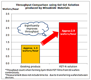
By using this new mass production technology, now users can obtain Mitsubishi Materials' sol-gel (PZT-N) solution through the 80EX spin coater designed by SCREEN Semiconductor Solutions. The coating frequency has been significantly reduced to a current number of 10 times from 20-30 times*4 before, through increasing thickness of coating films and performing uniform coating and baking processes on large surfaces.
This new mass production technology enables users to enjoy a remarkable improvement in productivity, as it has improved the throughput per one spin coater to 2.9 wafers/hour, more than two times the previous processing speed of 1.3 wafers/hour.
Also, wafers can now support a maximum 200mm size in MEMS applications.
3.Future Outlook
Thanks to this new mass production technology that combines the PZT sol-gel solution of Mitsubishi Materials with the spin coater handled by SCREEN Semiconductor Solutions, PZT films shall be produced early and easier at a practical level.
With the provision of this new mass production technology, Mitsubishi Materials and SCREEN Semiconductor Solutions will continue to contribute to the further development of MEMS devices.
The results of this new mass production technology will be reported at the “PiezoMEMS 2014” International Workshop on Piezoelectric MEMS, to be held in Kobe between October 28th and 29th this year.
Glossary of terms
- *(1) PZT (lead zirconate titanate) piezoelectric film:
Film of advanced material that produces a voltage when subjected to mechanical stress, while it distorts when subjected to a voltage. - *(2) MEMS:
Abbreviation for Micro Electro Mechanical Systems. Devices that integrate mechanical parts, sensors, actuators and electronic circuitry on a single substrate. - *(3) Sol-gel method:
Method to form a metal oxide film on a substrate through coating, drying and baking processes, by using a sol-gel solution containing organometallic compound. - *(4) Coating frequency to form a 2µm-thick PZT film, generally required for MEMS applications.
Image 1
Sol-Gel (PZT-N) solution
produced by Mitsubishi Materials
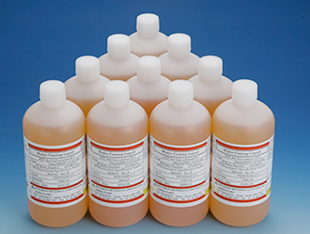
Image 2
Spin Coater (80EX)
produced by SCREEN Semiconductor Solutions
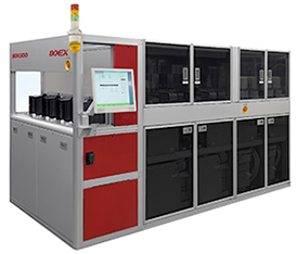
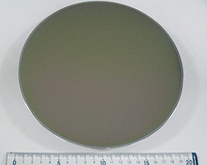
Image 3
2µm-thick PZT film formed on a 200mm wafer
Throughput Comparison
Mitsubishi Materials Corporation - Company Profile:
- Company Name
- Mitsubishi Materials Corporation
- Head Office
- 1-3-2 Otemachi, Chiyoda-ku, Tokyo
- Corporate Website
- http://www.mmc.co.jp/corporate/en/index.html
SCREEN Semiconductor Solutions - Company Profile:
- Company Name
- SCREEN Semiconductor Solutions Co., Ltd.
- Head Office
- Tenjinkita-machi 1-1, Teranouchi-agaru 4-chome, Horikawa-dori, Kamigyo-ku, Kyoto
- Corporate Website
- http://www.screen.co.jp/eng/spe/index.html
Inquiries about products
Mitsubishi Materials Corporation
Sales Dept. Advanced Materials Div. Electronic Materials & Components Company,
+81-3-5819-7320
+81-3-5819-7321
1-6-1 Yokoami, Sumida-ku, Tokyo, 130-0015 JAPAN
SCREEN Semiconductor Solutions Business Planning Dept.
+81-75-417-2527
+81-75-417-2546
Tenjinkita-machi 1-1, Teranouchi-agaru 4-chome, Horikawa-dori, Kamigyo-ku, Kyoto, 602-8585 JAPAN